
Precision Copper & Metal Stamping Solutions
Explore custom OEM engineered stamping components, high-current lug terminals, structural brackets, and specialized assemblies built to exact customer drawings.
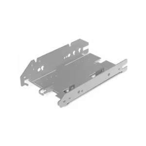
ODM Custom Precision Sheet Metal Brackets & Stamping Parts for Electronic Devices
View Product Details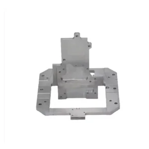
ODM High-Precision CNC Machined Metal Brackets & Structural Frames
View Product Details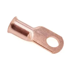
High-Quality Custom Tinned Copper Lug Ring Crimp Terminal Connector
View Product Details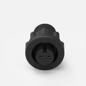
China Industrial IP67 2-Pin Waterproof Circular Connector (Nylon Series)
View Product Details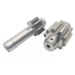
Custom CNC Machined Automotive Transmission Spur Gears & Gear Shafts
View Product Details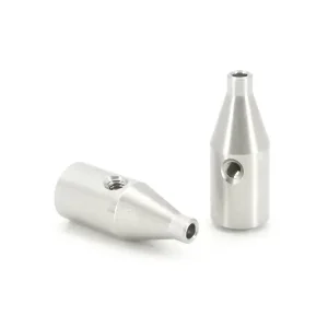
ODM Custom CNC Turned Aluminum Nozzle & Adapter Bodies Manufacturer
View Product Details
OEM High-Precision CNC Machined Metal Brackets & Frames for Aerospace
View Product Details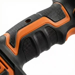
Dual-Material Power Tool Handle with Two-Shot Injection Molding
View Product DetailsThe Global Commercial & Industrial State of Copper Stamping Parts
Analyzing the pivotal role of pure copper and high-copper alloy precision stamped components in driving next-generation global electrification, AI computing infrastructure, and energy transition networks.
1. Macro Demand Drivers: Electrification, High-Frequency Computing, and Power Density
The global copper metal stamping market is undergoing an unprecedented structural expansion. As global manufacturing shifts toward decarbonization, high-efficiency power distribution, and artificial intelligence hardware, pure copper (C11000 ETP and C10200 OFHC) and specialty copper alloys (such as Beryllium Copper C17200 and Phosphor Bronze C5191) have become non-negotiable foundation materials. Precision copper stamped parts serve as the primary electromechanical interface in modern engineering, responsible for transmitting extreme electrical currents while managing critical thermal loads.
In high-power industrial electronics, electric vehicle (EV) traction systems, and hyper-scale data centers, component requirements have surpassed traditional stamping parameters. Global procurement executives and engineering directors no longer look for simple punch-press vendors; they require engineering partners capable of managing grain boundaries, controlling thermal annealing cycles, reducing burr heights below 5% of material thickness, and guaranteeing contact force retention across millions of operational micro-cycles.
Engineering Insight: Information Gain on Copper Alloy Selection
Choosing between C11000 (Electrolytic Tough Pitch) and C10200 (Oxygen-Free High Conductivity) copper requires balancing cost against hydrogen embrittlement risks during brazing or high-temperature glass-to-metal sealing. For spring contact terminals, replacing standard brass with C17200 Beryllium Copper increases yield strength up to 1400 MPa while maintaining superior stress relaxation resistance up to 200°C.
2. Material Science and Metallurgy Matrix in OEM Copper Stamping
Modern OEM copper stamping requires a deep metallurgical understanding of work hardening, grain orientation, and electrical conductivity trades-offs. Below is the technical breakdown utilized by top-tier engineering teams to match copper alloy grades with real-world application environments:
| Alloy Grade | UNS Number | Electrical Conductivity (% IACS) | Tensile Strength (MPa) | Primary Industrial Application |
|---|---|---|---|---|
| Electrolytic Tough Pitch (ETP) | C11000 | 100 - 101.5% | 220 - 380 | Power distribution busbars, switchgear contacts, high-current lug terminals. |
| Oxygen-Free Copper (OFHC) | C10200 / C10100 | 101% | 200 - 360 | Vacuum electronics, glass-to-metal seals, hydrogen-rich environment contacts. |
| Beryllium Copper (BeCu) | C17200 | 22 - 28% | 1100 - 1400 | High-reliability spring clips, micro-switches, aerospace battery interconnects. |
| Phosphor Bronze | C5191 / C5210 | 13 - 15% | 450 - 720 | PCB connectors, leaf springs, micro-stamped terminal pins. |
| CuNiSi High-Strength Alloy | C70250 | 40 - 50% | 650 - 800 | Automotive lead frames, high-temperature terminal crimps, AI server sockets. |
China's Ecosystem Efficiency in Precision Copper Stamping
Why leading global enterprises partner with Chinese OEM stamping factories to optimize tooling turnaround, achieve micron-level repeatability, and reduce total cost of ownership (TCO).
Rapid Progressive Tooling Velocity
Chinese stamping hubs integrate CAD/CAM design with high-speed wire EDM and CNC carbide grinding. Dies that take 8-12 weeks in Western facilities are engineered, tested, and validated (FAI) in 14-21 days.
- In-house Class-A carbide die manufacturing
- Multi-stage progressive & deep draw tooling
- Tooling life up to 50,000,000 continuous strokes
Integrated Surface Finishing Clusters
Local industrial supply chains physically integrate precision stamping facilities with automated electroplating lines (tin, selective gold, matte nickel, silver), eliminating cross-regional logistics delays.
- Continuous reel-to-reel plating lines
- XRF plating thickness verification (ISO 3497)
- Zero-discharge environmental compliance
AI-Assisted Quality Assurance
Advanced Chinese factories deploy high-speed optical vision systems directly on progressive stamping presses to inspect 100% of stamped copper terminals at speeds exceeding 800 parts per minute.
- In-line sensor detection for pitch variance
- Automated burr height monitoring system
- Zero defect (PPM < 10) quality guarantee
Precision Copper Metal Stamping Methodologies
Selecting the optimal cold-forming process for custom geometry, high conductivity requirements, and ultra-tight tolerances.
DFM & Moldflow
Computer simulation of strip layout, shear zone stress, and springback angle compensation for pure copper grades.
Tooling Precision
Wire EDM cutting of tungsten carbide punch insert components with sub-micron surface roughness finishes.
High-Speed Stamping
Execution on 25T to 300T precision tonnage presses featuring dynamic stroke balancing and thermal stability control.
Plating & Passivation
Continuous reel-to-reel electroplating of tin, silver, or gold to prevent copper oxidation and optimize solderability.
CMM & FAI Metrology
Complete dimensional inspection report generation including CPK evaluation, tension force, and conductivity validation.
Detailed Breakdown: Progressive Stamping vs. Deep Drawing Copper Components
Understanding when to implement Progressive Die Stamping versus Deep Drawing is critical for engineering cost optimization. Progressive stamping excels at complex, multi-feature geometry requiring high-speed bending, piercing, coining, and tapping within a single integrated tool block. It is ideal for battery contact clips, PCB shield cans, and intricate male/female spade connectors.
Conversely, Deep Drawing of copper is utilized when manufacturing seamless, cylindrical, or box-shaped hollow enclosures such as sensor caps, RF shielding cans, and motor housing shells. Deep drawing pure copper requires specialized lubricant management and multi-stage reduction steps to prevent material thinning and tearing due to copper's low strain-hardening exponent in soft tempers.
Industrial Application Scenarios for OEM Copper Stamping
Engineering tailored copper component solutions for mission-critical operating environments across five core global industries.
Electric Vehicles & Battery Packs
Flexible laminated copper busbars, battery cell interconnect rings, high-voltage battery disconnect terminals, and EV charging plug contact pins.
AI Servers & Telecom Hardware
Precision stamped copper vapor chamber heat spreader plates, backplane connector sockets, EMI/RFI PCB shielding frames, and high-speed signal contact pins.
Industrial Automation & Smart Grid
Heavy-duty circuit breaker contacts, transformer lugs, thermal overload relay blades, and micro-switch leaf springs manufactured from work-hardened copper alloys.
Emerging Trends & Global Sourcing Standards
Key technological advancements reshaping the precision copper metal stamping industry through 2030 and beyond.
1. Multi-Material Clad Metal Stamping (Copper-Aluminum & Copper-Steel)
To reduce overall assembly weight and optimize raw material costs without degrading electrical conductivity, leading OEM buyers are adopting clad strip materials. By cold-roll bonding copper to aluminum (Cu-Al) or copper to stainless steel (Cu-SS), progressive stamping dies can produce lightweight busbars and battery terminals where pure copper is localized solely at the critical contact faces.
2. Micro-Stamping and Ultra-Thin Foil Processing
The miniaturization of wearable devices, medical sensors, and silicon photonics packaging requires stamping pure copper foils down to 0.02mm (20 microns) thickness. Achieving clean sheared edges without material buckling demands sub-micron clearance die sets, temperature-controlled stamping presses, and cleanroom vacuum packaging.
3. Green Manufacturing & Closed-Loop Scrap Recycling
With stringent global carbon accounting (CBAM and ESG directives), OEM copper buyers are requiring closed-loop scrap recovery systems. High-tier Chinese stamping facilities segregate pure C11000 and alloy scrap at the press side, returning un-contaminated stamping skeletons directly to smelters to maintain supply chain transparency and achieve up to 98% material utilization efficiency.
Custom Precision Stamped & Machined Assemblies
Explore additional high-precision OEM products produced across our integrated stamping, CNC turning, and custom hardware manufacturing lines.
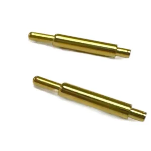
ODM High-Precision Gold-Plated Brass Pogo Pins for PCB Custom Connectors
View Product Details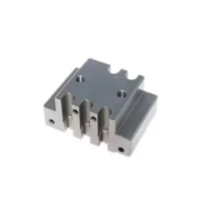
Custom OEM Precision CNC Machining Aluminum Industrial Components
View Product Details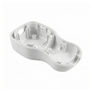
OEM Custom Medical Device Housing Precision Manufacturing Supplier
View Product Details
OEM Custom Precision Sheet Metal Brackets & Stamping Parts for Electronics
View Product Details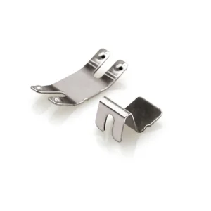
ODM Custom Precision Sheet Metal Stamping Clips & Electronic Hardware
View Product Details
Custom CNC Machined Spur Gears & Gear Shafts for Automotive Transmission
View Product Details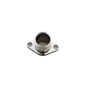
Premium Custom Stainless Steel Investment Casting for Valves & Impellers
View Product Details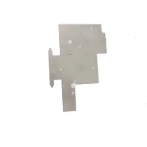
High-Quality Custom Laser Cut & Welded Heavy Equipment Control Panels
View Product DetailsFrequently Asked Questions: OEM Copper Stamping Sourcing
Comprehensive answers to common technical, metallurgical, and supply chain queries raised by procurement managers and structural design engineers.
How do you prevent burr formation during high-speed copper stamping?
Pure copper is soft and highly ductile, making it prone to burr creation and edge rollover during punching. We mitigate burrs by maintaining ultra-tight punch-to-die clearances (typically 3% to 5% of material thickness for copper), utilizing micro-grained carbide die components with diamond-like carbon (DLC) coatings, and implementing active oil lubrication during high-speed press runs. Furthermore, our optical sensors inspect burr heights continuously to ensure they remain strictly within the standard limit (<0.02mm or 5% of stock thickness).
What electroplating finishes are recommended for electrical copper terminals?
The choice of plating depends on operating temperatures and environmental exposure. Electro-tin plating (matte or bright, 3–8 microns) is standard for low-cost solderability and corrosion resistance. Selective silver plating (5–12 microns) is preferred for high-current automotive EV connectors to prevent fretting corrosion and handle high contact temperatures without thermal degradation. Selective gold plating over a nickel strike barrier is specified for micro-signal PCB terminals requiring low contact resistance over millions of insertion cycles.
How do you guarantee springback control in bent copper parts?
Because copper alloys exhibit variations in temper (from 1/4 hard to extra hard), springback angles can fluctuate between coil batches. We utilize finite element analysis (FEA) DFM simulation software to calculate exact springback allowances. In the progressive die, we incorporate secondary coining or over-bending stations that set the material's internal stress state, achieving stable bend angle tolerances within ±0.5° across batch runs.
What quality documentation accompanies custom OEM copper stamping shipments?
Every shipment is fully traceable and includes: 1) Raw Material Mill Certificates verifying chemical composition and IACS electrical conductivity; 2) First Article Inspection (FAI) reports with complete ballooned drawing dimensions; 3) Coordinate Measuring Machine (CMM) and optical measurement data; 4) Plating thickness measurement reports (XRF tested); 5) RoHS and REACH compliance statements.
What is the typical lead time for custom progressive stamping die tooling?
Prototypes and soft tooling (laser cutting + CNC forming) can be delivered in 3 to 5 business days for immediate design validation. Production-ready progressive carbide dies typically take 14 to 21 calendar days from final 3D CAD approval to First Article Sample submission. Mass production begins immediately upon FAI sign-off, with press speeds up to 800+ strokes per minute.
How is client intellectual property (IP) and CAD design data protected?
We enforce strict corporate IP confidentiality protocols. A legally binding Non-Disclosure Agreement (NDA) is signed prior to evaluating any 2D/3D customer drawings. CAD data is processed on secure engineering servers, and all production tooling is permanently assigned unique serial identifiers, remaining the exclusive property of the client.
Ready to Scale Your Copper Stamping Production?
Submit your 3D CAD files (STEP, IGES, DXF) or physical sample specifications today. Our engineering team provides comprehensive DFM feedback and transparent factory-direct pricing within 24 hours.