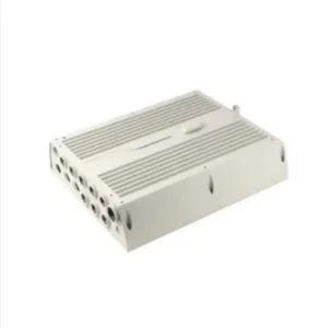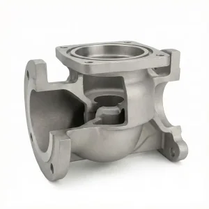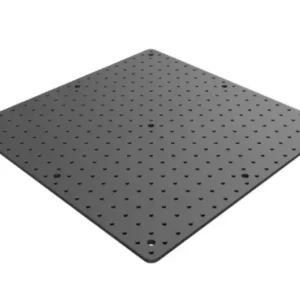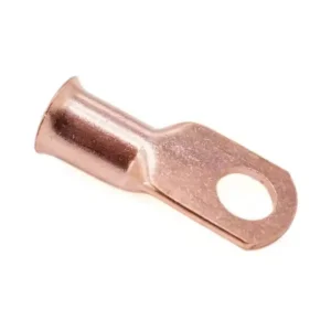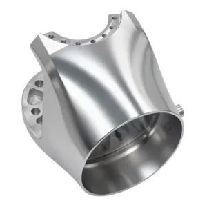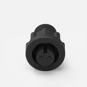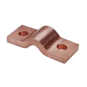
Featured High-Precision Stamping & Hardware Solutions
1. Global Macroeconomic Landscape & Evolution of Precision Metal Stamping
The global industrial sector is undergoing a profound paradigm shift driven by miniaturization, electrification, and structural lightweighting. High-precision metal stamping has evolved from a traditional mechanical shearing and forming process into a highly sophisticated, data-driven manufacturing discipline. Modern precision stamping services in China operate at the intersection of material science, sub-micron tool design, real-time sensor monitoring, and automated high-speed press engineering.
Global original equipment manufacturers (OEMs) across North America, Europe, and Asia-Pacific face mounting pressures to deliver next-generation products with tighter tolerances, higher structural integrity, and lower total cost of ownership (TCO). Whether producing ultra-thin EMI shielding enclosures for artificial intelligence (AI) server racks, flexible laminated copper busbars for electric vehicle (EV) battery packs, or micro-surgical titanium housing units, procurement leaders require manufacturing partners with proven engineering expertise and comprehensive quality assurance protocols.
EV & Clean Energy Transition
The rapid shift toward electric vehicles and renewable grid storage demands high-amperage conductive busbars, battery pack interconnections, and high-frequency shielding components stamped from copper alloys with zero burr thresholds.
AI Hardware & Telecommunications
High-density data centers require precision-stamped rack-mount PDU enclosures, heat sinks, and RF-shielding cans designed to withstand high thermal loads while maintaining precise electromagnetic isolation.
Medical Device Miniaturization
Next-generation diagnostic housing, implant connectors, and surgical instrumentation demand surgical-grade stainless steel and titanium micro-stamping with biocompatible surface finishes and absolute dimensional repeatability.
Information Gain Insight: The Metric That Matters
Piece-price procurement models are obsolete. Industry 4.0 buyers evaluate "Cost per Conforming Assembly" (CCA), which accounts for tool lifespan, downstream line-stoppage risks, scrap rate reductions, and automated quality control integration. China's advanced precision stamping ecosystem offers unmatched value when evaluated through this holistic metric.
2. Technical Deep-Dive: Progressive Die Tooling, Deep Drawing & Servo Press Technologies
Precision metal stamping is not merely punching holes into sheet metal; it is the controlled elastic and plastic deformation of crystalline metal structures under extreme tonnage. Achieving tolerances as tight as ±0.005 mm requires a comprehensive understanding of tool kinematics, springback compensation, and shear-band propagation.
Key Stamping Methodologies Comparison
Different geometric profiles and production volumes require specific tooling architectures. The table below outlines the primary stamping methods utilized in advanced Chinese manufacturing facilities:
| Stamping Methodology | Primary Geometric Output | Typical Material Thickness | Tolerance Capability | Optimal Production Volume |
|---|---|---|---|---|
| Progressive Die Stamping | Complex multi-feature terminals, connectors, contact springs | 0.05 mm – 3.0 mm | ±0.005 mm – ±0.02 mm | 50,000 to 10,000,000+ units |
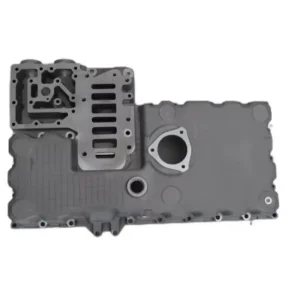
| Deep Drawing Stamping | Seamless cylindrical/rectangular cans, sensor housings, oil pans | 0.2 mm – 4.0 mm | ±0.015 mm – ±0.05 mm | 25,000 to 1,000,000+ units |
| Compound Die Stamping | Flat, high-precision washers, optical breadboard plates, shims | 0.1 mm – 6.0 mm | ±0.010 mm | 10,000 to 250,000 units |
| Servo Press Fine Blanking | Thick structural brackets, automotive gears, clutch components | 2.0 mm – 12.0 mm | ±0.008 mm (100% clean-cut edge) | 50,000 to 2,000,000+ units |
Sub-Micron Tooling Mechanics & Material Selection
The longevity and repeatability of a stamping operation depend entirely on progressive die construction. Leading Chinese stamping suppliers utilize tungsten carbide inserts, SKD11, and DC53 die steels hardened through vacuum heat treatment and cryogenic tempering to HRC 60-64.
- Tungsten Carbide Punch Strips: Essential for high-speed micro-stamping of abrasive beryllium copper and nickel-plated alloys, ensuring tool life exceeding 50 million strokes.
- In-Die Sensing Integration: Embedded optical and piezoelectric sensors measure slug lifting, strip pitch variation, and shut-height changes in real time, automatically halting presses before die damage occurs.
- Finite Element Analysis (FEA) Simulation: Prior to steel cutting, CAD drawings undergo rigorous AutoForm or PAM-STAMP simulations to predict material thinning, wrinkling, and elastic springback, reducing prototype turnaround times by up to 60%.
3. China’s Industry 4.0 Transformation: Supply Chain Resilience & Speed Advantage
China’s manufacturing landscape has transitioned from high-volume labor-intensive production to automated, digitalized Industry 4.0 smart factories. The concentration of integrated supply chains—specifically in regions like Shenzhen, Dongguan, and the broader Pearl River Delta—creates a distinct competitive advantage for international procurement teams.
Vertical Supply Chain Density
Raw material providers, heat treatment specialist shops, electroplating (gold, nickel, tin, anodizing), and CNC secondary machining facilities operate within a 30-minute radius, drastically shortening cycle times.
Closed-Loop Quality Control
Fully automated visual inspection systems (AOI) mounted directly onto stamping presses inspect 100% of critical dimensions at speeds up to 1,200 parts per minute, eliminating human error in defect detection.
Agile Tooling Lead Times
By pairing high-speed wire EDM with 5-axis CNC machining centers, Chinese mold shops can produce complex progressive stamping dies in 3 to 4 weeks—compared to 8 to 12 weeks in Western markets.
Material Engineering & Metallurgical Control
A key pillar of reliable precision stamping is raw material integrity. High-performing Chinese suppliers enforce stringent incoming inspection protocols, verifying raw coils using X-ray Fluorescence (XRF) spectrographic analysis and tensile strength testing. Standard supported materials include:
- Copper & Brass Alloys: C1100 Electrolytic Tough Pitch (ETP) Copper, C1020 Oxygen-Free Copper, Beryllium Copper (C17200), and Phosphor Bronze (C5191) for maximum electrical conductivity and fatigue resistance.
- Stainless Steels: SUS301 (full hard for spring contacts), SUS304, SUS316L (medical grade), and 430 magnetic stainless steel.
- Aluminum Alloys: AL1050, AL3003 (deep drawability), AL5052, and structural AL6061-T6.
- Exotic & High-Strength Steels: Titanium Grade 2 / Grade 5, Kovar, Invar, and DP780 Dual-Phase Ultra-High-Strength Steel for automotive crash safety structural members.
4. Global Enterprise Procurement Criteria: Assessing Supplier E-E-A-T
Evaluating custom metal stamping factories in China requires a systematic audit strategy focused on Experience, Expertise, Authoritativeness, and Trustworthiness (E-E-A-T). Sourcing managers must look beyond glossy website media and scrutinize measurable operational standards:
1. Design for Manufacturability (DFM) Engagement
A top-tier OEM factory does not simply accept CAD files; they provide thorough DFM analysis within 24 hours. This includes identifying sharp internal radii that cause stress concentration, proposing minor web-width adjustments to optimize coil layout utilization (reducing material scrap by 15-30%), and recommending appropriate grain direction alignment for bent features to prevent micro-cracking.
2. Traceable Quality Documentation & PPAP Level 3
For critical automotive, aerospace, and medical programs, production authorization demands full Production Part Approval Process (PPAP) submission, including:
- First Article Inspection Report (FAIR): Complete dimensional validation matching ballooned 2D engineering drawings via Coordinate Measuring Machines (CMM).
- Material Test Reports (MTR): Mill certificates tracing chemical composition and mechanical yield strength back to the heat lot number.
- Process Capability Studies (Cpk): Demonstration of key parameter Cpk values exceeding 1.67 over sustained production trials.
- RoHS / REACH Compliance: Certified chemical analysis verifying the total absence of restricted hazardous substances.
3. Intellectual Property (IP) Protection Protocols
Trustworthy manufacturers execute formal Non-Disclosure Agreements (NDAs) prior to receiving proprietary CAD files. Furthermore, advanced facilities maintain segmented IT networks, isolated production cells, and strict factory access control to safeguard customer IP from unauthorized disclosure.
5. Cross-Industry Applications & Case Analysis
Precision stamping products serve as structural backbones and electrical conductors across virtually every advanced manufacturing sector:
Automotive & EV Powertrain
High-voltage battery contact plates, sensor brackets, transmission clutch oil pans, laminated copper busbars, and terminal lugs designed for extreme vibration environments.
Medical Diagnostic Equipment
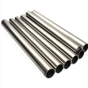
Titanium prosthetic connectors, stainless steel capillary tubing components, miniature sensor housings, and surgical instrument enclosures requiring cleanroom washing.
Industrial Controls & Data Centers
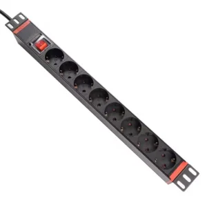
Rack-mount 16A PDU power strip assemblies, laser-cut heavy equipment control cabinets, optical breadboard sub-assemblies, and high-conductivity grounding clamps.
6. Comprehensive Quality Assurance & Metrology Architecture
Maintaining sub-micron consistency across millions of stamped components requires an uncompromising metrology infrastructure. Leading Chinese stamping manufacturers deploy state-of-the-art testing equipment within climate-controlled calibration laboratories:
CMM & 3D Laser Scanning
High-accuracy ZEISS Coordinate Measuring Machines verify complex 3D surface profiles, position tolerances, and hole centers down to sub-micron thresholds.
Salt Spray & Environmental Testing
Automated corrosion testing chambers evaluate plating durability (zinc, nickel, chrome, passivated stainless steel) up to 1,000+ hours of continuous salt fog exposure.
Electrical Conductivity & Plating Inspection
Eddy-current instruments measure %IACS copper conductivity, while X-ray fluorescence (XRF) gauges non-destructively measure micro-inch plating thicknesses.
7. Frequently Asked Questions by Global Engineering & Procurement Teams
Explore Specialized Hardware & Component Solutions