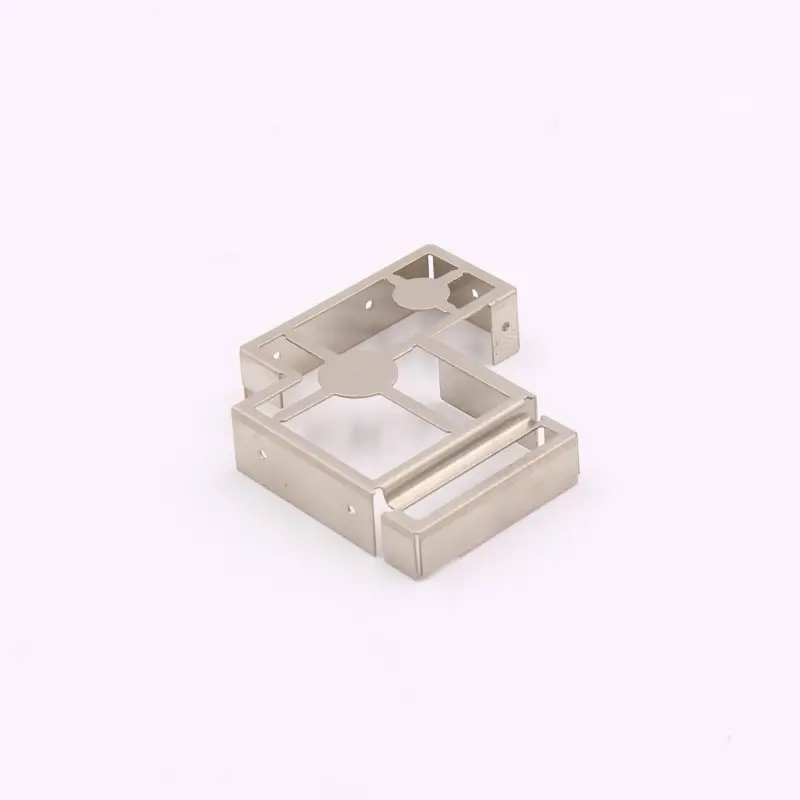
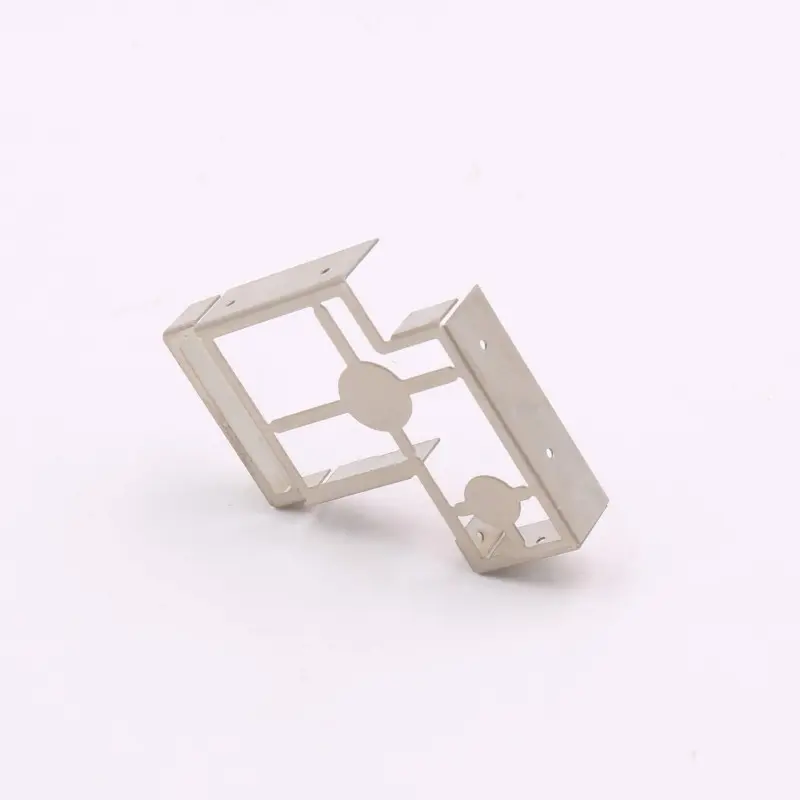
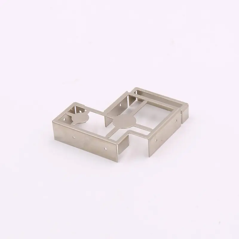
OEM Custom High-Precision PCB EMI/RFI Shielding Frame Manufacturer, Products
Product Description
Product Overview
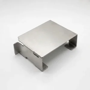
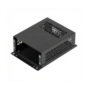
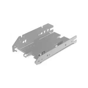
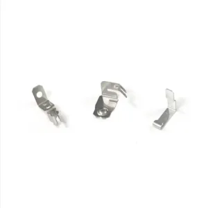
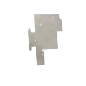
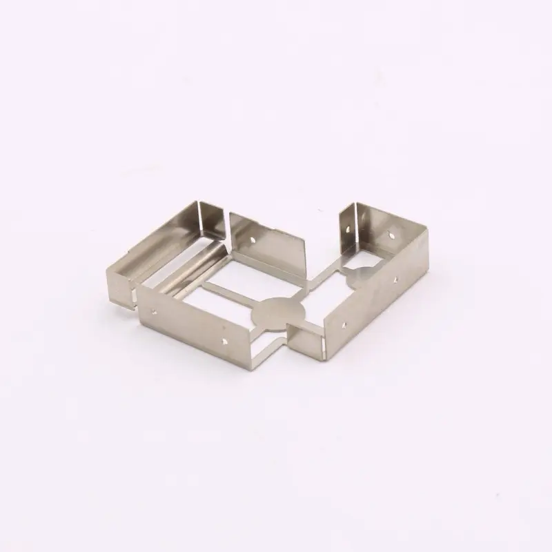
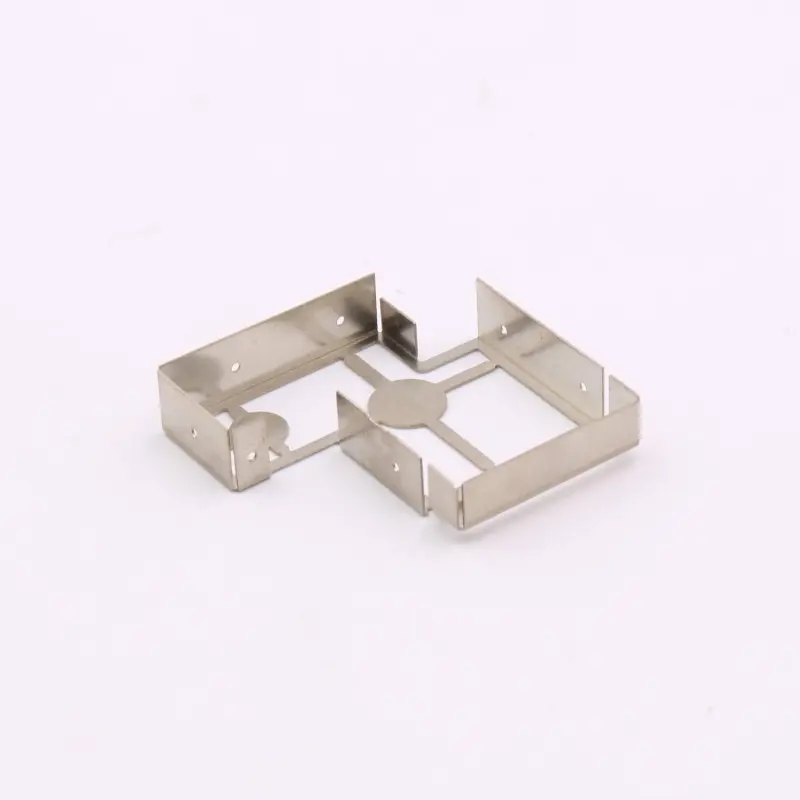
Shenzhen Sunmy Hardware Co., Ltd. specializes in engineering and manufacturing premium-grade, custom PCB EMI/RFI Shielding Frames (Shielding Cans). These components are vital for modern high-density electronic assemblies, serving to isolate sensitive RF/microwave circuits, microcontrollers, and wireless modules from electromagnetic interference (EMI) and radio-frequency interference (RFI), while preventing internal emissions from disrupting adjacent components.
Featuring an intricate multi-compartment architecture, custom geometric cutouts, and dedicated grounding/positioning pins, our shielding frames ensure seamless integration with automated Surface Mount Technology (SMT) pick-and-place lines. Built for superior co-planarity, durability, and high shielding effectiveness, these frames provide robust protection for demanding commercial, industrial, telecommunications, and automotive electronic ecosystems.
Process & Manufacturing Insights
Our manufacturing division leverages cutting-edge Precision Sheet Metal Stamping technology to achieve complex three-dimensional shapes with tight structural tolerances. The production lifecycle comprises:
-
Advanced Tooling & Progressive Dies: We design and build in-house progressive stamping dies engineered for high-volume repeatability, ensuring every batch maintains perfect structural alignment, flat surfaces, and crisp 90-degree bends without micro-cracking.
-
Precision CNC Bending & Forming: For complex geometries, low-volume validation phases, or rapid prototyping, advanced CNC forming machines are deployed to achieve excellent co-planarity (typically within ±0.05mm), preventing defects during reflow soldering.
-
Strategic Material Selection & Surface Finish: We utilize premium materials such as Nickel Silver (Cu-Ni-Zn alloy) for excellent native solderability and corrosion resistance without post-plating, as well as Tin-Plated Steel, Stainless Steel, and Brass. Surface finishes are strictly controlled to facilitate low electrical contact resistance and optimal thermal characteristics.
Technical Specifications
| Parameter / Property | Technical Standard / Capability | Customization Scope |
|---|---|---|
| Primary Manufacturing Process | Precision Sheet Metal Stamping / Progressive Die | 100% Tailored to customer tool design |
| Common Materials | Nickel Silver (C7701/C7521), Tin-Plated Steel, Stainless Steel (SUS301/304), Brass, Copper | Available upon request based on RF shielding needs |
| Material Thickness Range | 0.15 mm – 1.00 mm | Fully customizable based on structural requirements |
| Dimensional Tolerance | ±0.02 mm to ±0.05 mm (High Precision) | Strict adherence to critical-to-quality (CTQ) dimensions |
| Co-planarity Control | ≤ 0.08 mm (Standard SMT requirement) | Optimized down to ≤ 0.05 mm for ultra-fine pitch PCBs |
| Surface Finishing | De-greasing, Cleaning, Tin Plating, Nickel Plating, Selective Plating | Custom plating thickness and chemical cleaning protocols |
| Geometry & Layout | Multi-compartment walls, internal labyrinth ribs, thermal ventilation slots, positioning tabs | Completely configurable based on PCB component layout |
| Packaging Formats | Tape & Reel (EIA-481 standard), Matrix Tray, Bulk Pack | Configured for automated high-speed SMT pick-and-place lines |
Key Features & Strategic Advantages
-
Uncompromised Shielding Effectiveness: Engineered with meticulous continuous trace contacts and precision interlocking joints to eliminate RF leakage across multi-band wireless designs (5G, Wi-Fi 6E/7, Bluetooth, GPS).
-
100% Full Customization & DFM Support: We translate your STEP/IGES CAD layouts into production-ready designs. Our engineering team conducts thorough Design for Manufacturability (DFM) reviews to optimize tooling cost, material yield, and SMT assembly yield.
-
Superior Reflow Solderability: By utilizing high-grade raw materials and advanced chemical de-greasing cycles, our shielding frames eliminate oxidation risks, guaranteeing perfect solder wetting, robust mechanical joints, and minimal voiding.
-
Robust OEM/ODM Development & Tooling Capacity: Shenzhen Sunmy Hardware is a true manufacturing partner. From rapid CNC prototypes within days to complex multi-stage progressive stamping dies for millions of parts, our robust manufacturing infrastructure guarantees short lead times and stable supply chains.
Technical FAQ
Q1: What files and data are required to initiate a custom quotation?
A1: Please provide your 3D CAD models in STEP, IGES, or SolidWorks format, along with a detailed 2D engineering drawing indicating critical dimensions, material preference, thickness, and tolerancing requirements.
Q2: How does Sunmy Hardware guarantee tight co-planarity standards for SMT pick-and-place?
A2: We implement in-die sensor monitoring alongside automated optical inspection (AOI) systems and custom-made co-planarity gauge blocks. Standard production maintains co-planarity within ≤0.08mm, with specialized adjustments achieving ≤0.05mm for high-precision layouts.
Q3: What is the typical lead time for prototype tooling vs. mass production?
A3: Rapid prototypes using soft tooling or CNC laser + bending typically take 5 to 7 business days. Hard tooling / progressive production dies require 15 to 25 days depending on layout complexity, followed immediately by sample approval and high-speed mass production.
Q4: Do you offer flexible Minimum Order Quantities (MOQ)?
A4: Yes. We are dedicated to supporting your product development lifecycle. We offer flexible MOQs for initial engineering verification testing (EVT) and design validation testing (DVT) phases before scaling up to high-volume commercial production batches.
Q5: Which surface finishing options provide optimal solderability and corrosion resistance?
A5: We provide raw Nickel Silver for direct reflow soldering without additional plating, as well as electrolytic Tin Plating, Selective Gold Plating, and Nickel Plating to ensure minimal contact resistance and long-term shelf-life protection.
Q6: Can you manufacture multi-compartment EMI frames for complex PCB layouts?
A6: Yes, our progressive tooling allows custom multi-compartment internal wall configurations, enabling isolated shielding for multiple RF/digital components within a single structural frame to optimize PCB real estate.
Other Products
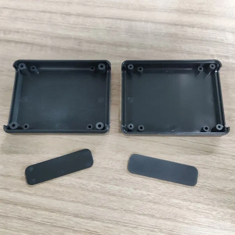
Custom Modular Plastic Enclosures
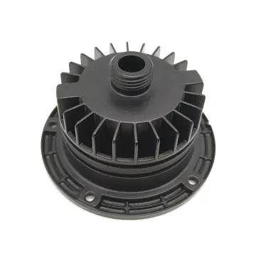
Custom Die Cast Aluminum Finned Housings
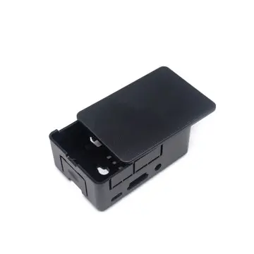
Custom Injection Molded Electronics Enclosure
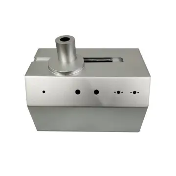
Custom Precision Sheet Metal Enclosure
Get a Fast, Technical Quote & Free DFM Review
Don't let tolerance stack-up delay your product launch. Submit your project details, and our engineering team will evaluate your design for manufacturability before the first cut.