
Featured Hardware Stamping & Machined Products
Explore our custom precision components produced via progressive die stamping, CNC turning, and advanced metallurgy.
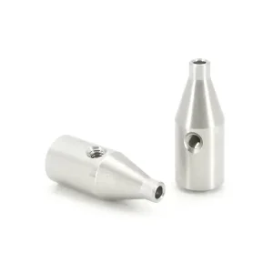
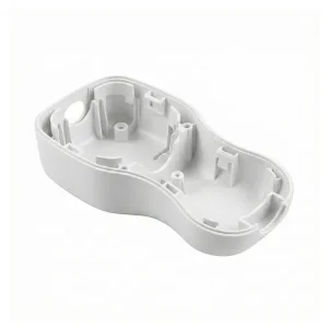
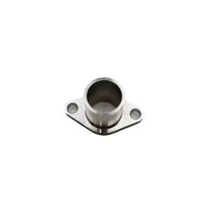
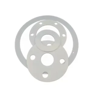
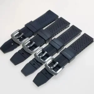
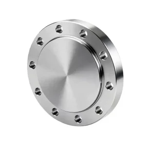
State of Modern Hardware Stamping Manufacturing
Precision metal stamping remains the cornerstone of modern industrial manufacturing, converting raw sheet metal coils into highly complex, structural, and conductive components with microscopic repeatability.
In high-stakes industries such as automotive e-mobility, aerospace avionics, medical diagnostics, and 5G telecommunications, standard manufacturing tolerances are no longer sufficient. Hardware stamping manufacturers must now operate at the intersection of metallurgical science, sensor-integrated tooling, and dynamic springback algorithm modeling.
This whitepaper outlines the structural parameters, technical methodologies, and operational paradigms that define top-tier custom metal stamping, progressive die engineering, and contract assembly.
Global Commercial & Industrial Hardware Stamping Landscape
Analyzing global shifts in precision component demand, material availability, and OEM localized integration.
North American Automotive & Energy
The acceleration of North American EV manufacturing and renewable grid infrastructure has created unprecedented demand for complex copper busbars, battery pack structural shieldings, and high-current terminal contacts requiring strict C11000/C12200 alloy compliance.
European Precision & Medical Standards
European OEMs prioritize strict environmental compliance (RoHS 3, REACH SVHC) alongside micron-level dimensional stability for medical diagnostic housings, surgical stapler jaws, and miniaturized sensor enclosures made from medical-grade 316L stainless steel.
Asia-Pacific High-Density Electronics
As the world's epicenter for consumer hardware and telecom infrastructure, Asia-Pacific drives innovation in micro-stamping EMI/RFI shielding cans, beryllium-copper battery contacts, and ultra-thin server chassis assemblies designed for maximum thermal dissipation.
Tooling Process Selection & Material Specifications
Choosing the optimal stamping architecture (Progressive vs. Transfer vs. Deep Drawing) based on volume, geometric complexity, and grain orientation.
| Stamping Process | Ideal Application | Tolerance Standard | Material Thickness Range | Key Advantage |
|---|---|---|---|---|
| Progressive Die Stamping | High-volume intricate terminals, EMI shields, brackets | ±0.010 mm to ±0.025 mm | 0.10 mm – 3.50 mm | Maximum throughput, lower piece price, multi-operation feed |
| Deep Drawing Stamping | Cylindrical cans, motor housings, medical canisters | ±0.015 mm to ±0.030 mm | 0.20 mm – 4.00 mm | Seamless wall geometries, excellent structural integrity |
| Transfer Die Stamping | Large structural automotive frames, heavy chassis panels | ±0.025 mm to ±0.050 mm | 1.00 mm – 8.00 mm | Large component versatility, individual blank manipulation |
| Micro Stamping | Medical contacts, micro-connectors, sensor pins | ±0.005 mm to ±0.012 mm | 0.02 mm – 0.50 mm | Micron precision, extreme edge quality, minimal burr |
Localized Application Scenarios across Strategic Sectors
Engineered hardware stamping solutions designed to withstand rigorous field environments and stress cycles.
Automotive & Powertrain
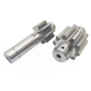
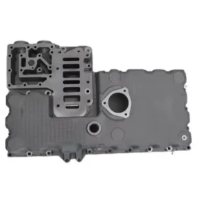
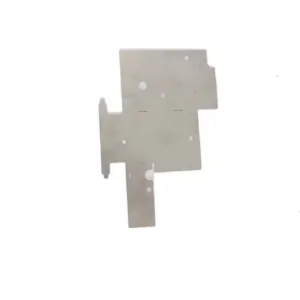
High-reliability retarder plates, transmission gear shafts, clutch oil pans, and battery interconnect busbars tested for thermal shock, vibrational resonance, and mechanical fatigue.
Medical Devices
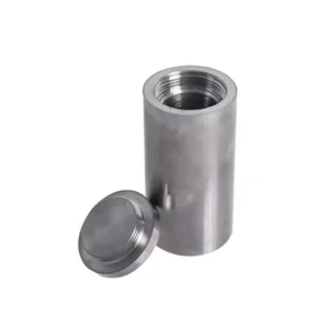
Titanium and stainless steel custom medical housings, surgical tool components, and shielded canisters manufactured in cleanroom environments with full bio-compatibility testing.
Server & Cloud Telecom
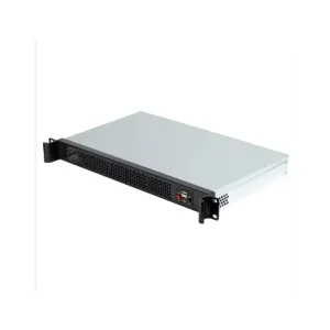
1U/2U rackmount chassis enclosures, high-density heat sink clips, EMI shielding covers, and gold-plated copper alloy battery contacts for uncompromised signal fidelity.
Heavy Industrial Panels
Laser-cut, deep-drawn, and welded heavy equipment control panels, water valve impellers, structural brackets, and high-pressure pipe fittings engineered for harsh outdoor environments.
Technology Roadmap: Industry 4.0 in Metal Stamping
How real-time sensor integration and green metallurgy are redefining component quality through 2030.
Smart IoT In-Die Sensing
Integration of piezoelectric force sensors, acoustic emission detectors, and thermal monitors directly inside progressive dies to catch micro-cracks, burr elevation, and material misfeeds instantaneously.
AI Optical Vision Inspection
Automated inline high-speed camera systems capable of performing 100% 3D surface defect and key-dimension checks on up to 1,200 stamped parts per minute, eliminating human error.
Sustainable Metallurgy & Recycling
Closed-loop scrap segregation protocols that return 99.8% of raw aluminum, copper, and stainless steel trimmings directly back to certified mills, significantly reducing carbon footprint.
China Factory Supply Chain Resilience & Speed
Leveraging the Shenzhen Hardware Ecosystem for Rapid Tooling, Scale, and Cost Efficiency.
Located in Shenzhen, Guangdong—the world’s premier industrial manufacturing center—our facility integrates the entire hardware supply chain within a 30-kilometer radius. From raw material sourcing to precision tooling design, surface plating, and final inspection, our operations offer unmatched agility.
- Ultra-Fast T1 Sample Delivery: Tooling design to initial physical samples in as little as 10 to 14 working days using wire EDM and modular die blocks.
- Vertical In-House Capability: In-house CNC machining, metal stamping press lines (25-ton to 600-ton capacity), vacuum heat treatment, and surface plating.
- Comprehensive Material Stocking: Immediate access to certified SUS304/316, C1100 Copper, Phosphor Bronze, Titanium Grade 5, and Aircraft-grade Aluminum 6061/7075.
Quality Control Assurance Checklist
Every production batch undergoes strict quality gates prior to international dispatch:
Localization Support & Global Regulatory Compliance
Seamless international logistics, customs clearance, and global quality standards certification.
International Certifications
Operations strictly follow ISO 9001:2015 and IATF 16949 quality frameworks. Full compliance documentation including RoHS 3, REACH, and Conflict Minerals (3TG) statements provided with every order.
Door-to-Door (DDP/DAP) Delivery
Flexible logistics support including air express, sea freight, and dedicated rail container freight with full DDP (Delivered Duty Paid) custom clearance to North America, Europe, and Asia.
VMI & Safety Stock Buffers
We support Vendor-Managed Inventory (VMI), blanket order schedules, and localized safety stock buffering to protect your assembly lines against global shipping fluctuations.
Frequently Asked Questions (FAQ)
Engineering details regarding custom stamping die tooling, tolerances, surface treatments, and lead times.
What dimensional tolerances can your progressive die stamping achieve?
Our high-precision progressive stamping presses can routinely hold dimensional tolerances of ±0.010 mm (±0.0004 in) on high-volume production runs. For micro-stamping applications (such as electrical connector contacts or medical components), critical features can be maintained down to ±0.005 mm (±0.0002 in) using optical sensor feedback and carbide tooling inserts.
How do you prevent metal springback during deep drawing and bending?
Springback is mitigated during the preliminary Design for Manufacturability (DFM) phase using FEA algorithm simulation software. We engineer over-bending angles, add stiffening ribs/embossments into the tooling geometry, and adjust coining pressure to set residual stresses in the material deformation zone.
What surface finishing options are available in-house or through audited partners?
We offer comprehensive surface finishing including electroplating (gold, silver, tin, nickel, copper), anodizing (Type II & Type III Hardcoat), passivation, powder coating, electropolishing, e-coating, and custom laser etching for part traceability.
What is your typical lead time for custom stamping tooling and T1 samples?
Standard progressive die tooling fabrication and initial T1 sample delivery typically require 12 to 18 business days depending on die complexity. Rapid prototype samples produced via laser cutting and short-run soft tooling can be delivered in as few as 3 to 5 business days.
How does your factory protect customer IP and proprietary 3D CAD models?
Prior to receiving any CAD models, drawings, or engineering specifications, we execute a legally binding bilateral Non-Disclosure Agreement (NDA). All files are stored on isolated secure servers with restricted project-level access for assigned engineers only.
Additional Custom Stamping & Machining Assemblies
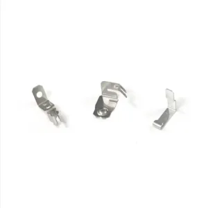
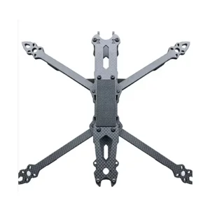
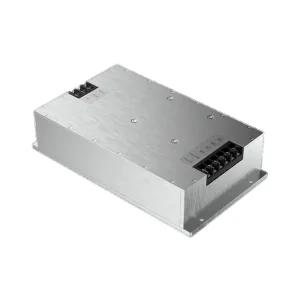
Explore our custom OEM hardware components engineered for heavy equipment, server racks, and drone frames.
Request a DFM Engineering Analysis for Your Project
Submit your 3D STEP/IGES files or 2D dimensioned drawings today. Our senior tooling engineers will respond within 24 hours with a comprehensive DFM review and competitive quote.