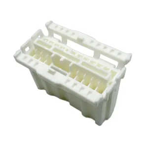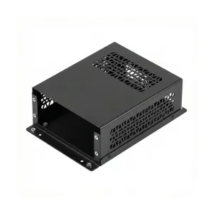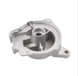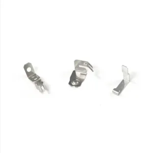
Featured Precision Stamping & Hardware Series
Explore our active production line products featuring advanced copper, aluminum, titanium, and composite engineering.
Engineering Principles of High-Precision Copper Metal Stamping
A deep dive into copper alloy selection, progressive die dynamics, grain boundary alignment, and springback control in mass production.
Advanced Copper Alloy Metallurgy
Copper (Cu) is praised for high electrical conductivity (>100% IACS) and superior thermal dissipation. Selecting the correct grade dictates stamped part durability:
- C11000 (ETP Copper): High electrical conductivity (101% IACS). Ideal for busbars, battery terminals, and transformer windings.
- C12200 (DHP Copper): Deoxidized high phosphorus copper, superior for deep drawing and brazed assemblies.
- C17200 (Beryllium Copper): Exceptional yield strength (>1100 MPa post heat treatment) and fatigue resistance for spring contacts.
- C5191 / C51000 (Phosphor Bronze): Optimal elasticity, wear resistance, and anti-corrosion properties for high-cycle connectors.
Progressive Tooling & Die Physics
Achieving tight tolerances (±0.005 mm) across millions of cycles demands precise punch-to-die clearances (typically 3% to 5% of material thickness for soft coppers). Tool design incorporates tungsten carbide inserts, high-speed steel (D2/SKD11) punches, and sensor-guided die protection to prevent misfeeds and galling.
Grain Alignment & Springback Mitigation
Pure copper exhibits pronounced directional elasticity along rolling lines. Our FEA-assisted DFM tooling simulates grain orientation to eliminate micro-cracks during 90-degree radius bends, utilizing over-bending and coin-stamping techniques to neutralize springback variations across material lots.
Copper Alloy Selection Matrix for OEM Engineers
Refer to our empirical material performance matrix when specifying raw stock for custom copper stamped parts:
| Grade / Alloy | UNS Code | Electrical Conductivity (% IACS) | Tensile Strength (MPa) | Primary Application Scenarios |
|---|---|---|---|---|
| Electrolytic Tough Pitch (ETP) | C11000 | 101% | 220 – 380 | EV Busbars, High-Current Power Terminals, Switchgear |
| Oxygen-Free Copper (OFC) | C10200 | 102% | 200 – 360 | Vacuum Electronics, Audio Interconnects, Semiconductor Leads |
| Phosphor Bronze (5% Sn) | C51000 / C5191 | 15% – 20% | 350 – 650 | Spring Terminals, Leaf Switches, Coin Cell Battery Contacts |
| Beryllium Copper (CuBe) | C17200 | 22% – 28% | 680 – 1250 | High-Reliability Aerospace Socket Contacts, Micro-Switches |
| Brass (70/30 Cartridge) | C26000 | 28% | 300 – 550 | Fasteners, Decorative Housings, Low-Voltage Connectors |
Why Shenzhen Sunmy Hardware Dominates Precision Copper Stamping
Combining regional industrial cluster advantages with internal digitalized quality control systems.
Supply Chain Density & Raw Material Sourcing
Situated in Shenzhen (Longgang District), Sunmy Hardware leverages direct relationships with premier copper rolling mills. This minimizes raw material lead times to 48 hours and ensures certified lot-to-lot consistency with complete melt-mill test certificates (MTC).
Rapid Prototype to High-Speed Tooling Iteration
Our in-house CNC wire-EDM and 5-axis milling centers enable short-run soft tooling for functional prototypes within 5 days, seamlessly converting into multi-cavity progressive dies capable of 400+ strokes per minute (SPM).
Multi-Tier Surface Finishing & Electroplating
Copper naturally oxidizes. We offer complete surface protection under one purchase order, including continuous reel-to-reel selectively plated Gold, Silver, Matte Tin, Bright Nickel, and Anti-Tarnish (Benzotriazole BTA) passivation.
Global Market Drivers Reshaping Copper Stamping Demand
Key structural shifts in energy transition, cloud data infrastructure, and smart automation.
1. Next-Gen EV Power Electronics & High-Voltage Busbars
With 800V EV architectures becoming standard, heavy-gauge copper busbars (1.5mm to 6.0mm thickness) require specialized press beds capable of high-tonnage precision coining, multi-angle bending, and over-molded insulation interfaces.
2. AI Data Centers & High-Frequency Shielding
AI compute clusters consume massive current while generating intense Electromagnetic Interference (EMI). Micro-stamped copper shielding cans and beryllium copper fingerstock gaskets ensure signal integrity across multi-gigahertz backplanes.
3. ESG, Recyclability & Circular Supply Chains
Global enterprises demand verified green supply chains. Copper is 100% recyclable without loss of performance. Sunmy implements closed-loop scrap recovery systems, reducing total carbon footprint across raw material sourcing.
Tailored Copper Stamping Solutions Across Key Sectors
From micro-miniature battery clips to heavy-duty industrial switchgear components.
Automotive & Battery Management (BMS)
Custom flexible copper shunts, cell interconnect busbars, fuse terminals, and sensor spade connectors engineered to withstand severe thermal cycling and high vibrational loads.
Consumer Electronics & Wearables
Ultra-thin phosphor bronze coin cell battery contacts (AG13, CR2032, CR2450), SIM card trays, antenna springs, and ultra-miniature surface-mount (SMT) clip terminals.
Telecommunications & Optical Networks
RF shield enclosures, board-to-board high-speed interconnect pins, grounding springs, and fiber optic transceiver housing retention brackets.
Medical & Surgical Devices
Precision electrical surgical contacts, fluid control valve components, diagnostic sensor strips, and biocompatible gold-plated connectors.
Industrial Automation & Smart Grids
Heavy-current breaker contacts, relay springs, transformer terminal block links, and DIN-rail mounting grounding clips.
Enterprise Procurement & Risk Mitigation Standard
How Shenzhen Sunmy Hardware guarantees compliance, zero-defect delivery, and intellectual property protection.
Procuring custom hardware from offshore suppliers requires strict quality verification frameworks. Sunmy Hardware operates an ISO-certified quality management system integrated into every production phase:
DFM & CAD Review
Comprehensive bend radius, thickness ratio, and tool access analysis before steel cutting.
Raw Material IQC
XRF alloy analyzer validation for chemical composition and electrical conductivity checks.
FAI & CMM Inspection
First Article Inspection backed by 2D optical measuring and 3D CMM dimension mapping.
In-Line AOI Monitoring
Automated optical vision systems inspecting burrs, pin pitch, and surface defects at full press speed.
RoHS / REACH Pack
Full material traceability documentation, plating thickness reports, and compliance certificates.
Strict IP Protection Guarantee
We execute legally binding Non-Disclosure Agreements (NDAs) prior to taking receipt of customer 2D/3D CAD models (STEP, IGES, DXF, PDF). Your proprietary designs are processed exclusively on isolated internal networks and never subcontracted to unauthorized third parties.
Frequently Asked Questions (FAQ)
Expert answers to common engineering, procurement, and tooling queries.
What is the difference between single-stage stamping and progressive die stamping for copper?
Single-stage (stage tooling) performs one operation per stroke (e.g., piercing or bending) and is best suited for low-volume prototypes or simple geometry. Progressive die stamping feeds a continuous copper strip through multiple sequential stations within a single die. It achieves extreme efficiency (up to 400+ strokes per minute), complex 3D forming, tighter tolerances, and significantly lower per-part costs during medium to high-volume production runs.
How does Sunmy Hardware control burrs on copper stamped parts?
Pure copper is soft and ductile, making it susceptible to burr formation during shearing. We manage burr height (holding it under 5% of material thickness) through precise punch-to-die clearances, ultra-sharp tungsten carbide tooling, micro-finish die sharpening, and automated post-processing options such as electro-polishing, chemical deburring, or barrel tumbling.
What surface plating options are recommended for electrical copper contacts?
Plating selection depends on electrical requirements and environment:
- Tin (Matte or Bright): Cost-effective solution providing good solderability and corrosion resistance. Ideal for PCB terminals.
- Silver: Excellent electrical conductivity for high-current busbars and switching contacts, though susceptible to tarnishing without passivation.
- Gold over Nickel: Premium choice for micro-contacts requiring low insertion force, zero oxidation, and exceptional wear life in harsh environments.
What file formats are accepted for DFM and quoting?
We accept 3D CAD models in STEP (.stp, .step), IGES (.igs), and Parasolid (.x_t) formats. For dimensional tolerances, thread specifications, and surface callouts, please provide native 2D drawings in PDF or DWG/DXF format alongside your 3D files.
What is the typical lead time for custom copper stamping tooling and production?
Prototype samples created via laser cutting and soft tooling can be delivered in 5 to 7 business days. High-speed progressive tooling development typically takes 18 to 25 days depending on part complexity. Once tooling is approved (FAI), mass production runs require 10 to 14 days.
Can you handle post-stamping heat treatment for Beryllium Copper (CuBe)?
Yes. Beryllium copper alloy C17200 is stamped in its ductile annealed state and subsequently age-hardened in controlled vacuum furnaces at approximately 315°C (600°F) to achieve maximum tensile strength, hardness, and spring memory without distorting critical part dimensions.
Explore More Precision Engineered Components
Cross-process hardware solutions manufactured to exact OEM specifications.